Blog & News
We upload to our blog every couple of weeks, sharing insightful articles from our engineers as well as company news an our opinions on recent industry topics. Subscribe to our mailing list to get great content delivered straight to your inbox.

What will the future of wafer fabrication look like? With innovative AI-driven technologies paving the way for significant improvements in efficiency, quality and on-time delivery whilst also driving down costs – chip manufacturers need to be paying close attention.
What will the future of wafer fabrication look like? With innovative AI-driven technologies paving the way for significant improvements in efficiency, quality and on-time delivery whilst also driving down costs – chip manufacturers need to be paying close attention. In SEMI's upcoming FutureFab Solutions webinar, we explain why disruptive technologies, such as the hybrid optimization-driven scheduling that Flexciton provides, are pivotal in making progress towards Industry 4.0. We will discuss the technology behind Flexciton’s solution as well as how it performed when it was deployed live into the photolithography area of a Seagate Technology wafer fab.
This webinar will be taking place on June 21 from 17:00–18:00 CEST (16:00–17:00 BST). Can't make it? The full session will also be available on-demand for those who register.
Here’s an overview of what we’ll be covering:
- Flexciton’s optimization-driven solution and the scheduling strategy they used when challenged with increasing capacity at Seagate’s Springtown facility.
- Real case studies presented by both Seagate and Flexciton on the results gathered from deployment into the photolithography area.
- How Flexciton’s advanced scheduling managed to enable an increase in throughput and a reduction in the amount of reticle moves.
This webinar is hosted by SEMI and will feature presentations from Flexciton, Seagate Technology and Lynceus AI, another disruptive AI-driven solution provider that will talk about their case study from deployment into a Tier 1 automotive supplying wafer fab.
You can register your space today by following this link: https://www.semi.org/eu/events/Future-Fab-Webinar

The semiconductor industry worries that it won’t have enough workers to run its new fabs. But there’s a labour problem right now at legacy facilities. Could disruptive technologies help to solve this problem?
The semiconductor industry worries that it won’t have enough workers to run its new fabs. But there’s a labour problem right now at legacy facilities. Could disruptive technologies help to solve this problem?
A worldwide labour crisis
It’s not just supply chain issues that are afflicting the semiconductor industry. Another major problem is a shortage of labour. There’s a significant fab building programme underway, but already companies fear there won’t be enough manpower to run them properly.
This is a worldwide issue. A recent white paper by talent management company Eightfold shows that, to meet the capacity demands from new fabs, the US chip industry needs to increase its workforce by at least 50%. And according to Deloitte, China is also facing a labour crisis, with 400,000 more semiconductor employees required to meet its stated targets. Even Taiwan is feeling the pinch, with a huge gap opening up between rocketing demand and the ability to meet it due to a lack of skilled engineers.
Unsurprisingly, these countries are doing everything they can to boost the number of STEM graduates, with billions of dollars going into universities to support this goal. In addition, the SEMI Foundation – the non-profit arm of global industry association SEMI – has a number of programmes in place to develop a larger and more diverse workforce, with the ultimate aim to dramatically expand the pipeline of skilled workers ready to fill labour deficits.
However, while these initiatives are laudable and entirely necessary, they don’t address the labour issues that many legacy fabs are facing right now. These issues – such as experienced operators retiring and skilled engineers being poached by newer, bigger facilities – mean that it’s growing ever harder for legacy fabs to meet capacity pressures. With their workforces dwindling or under threat, what can be done to ensure that legacy fabs are still able to operate efficiently?
The problem of running fabs on gut feeling
One solution is to change the way in which fabs operate. Many legacy facilities are still reliant on workers on the floor to move WIP from one machine to the next, since upgrading legacy fabs to facilitate advanced material handling systems (AMHS) is often too costly or too complicated. Instead, operators tend to take instructions from a rules-based scheduling software. However, in some instances the operators will make their own scheduling decisions based on their ‘gut feeling’ if, for example, the system doesn’t take into account certain constraints and makes an implausible suggestion or the operator thinks they can make a better decision themselves.
Because of the lack of intelligence in rules-based scheduling systems, many chip companies have to rely on experienced, highly-skilled operators to oversee the manufacturing process. Therefore, when companies look to expand facilities or replace employees, they understandably think they need to find operators experienced enough that they require minimal training to adapt to their fab – and worry that new candidates don’t exist in sufficient quantity.
However, if decision-making around scheduling in the fab can be improved, with less dependence on operators’ own judgements, then it’s possible to not onboard new staff much quicker but also optimize the total number of people needed to run the facility.
The simple rules-based scheduling software that many fabs rely on to guide operators’ decisions runs using predefined rules. These predefined rules take into consideration only a limited number of possible cases, resulting in the software making suboptimal decisions when it is faced with unknown scenarios which contribute to inconsistent results. Little wonder then that experienced operators often believe their own scheduling decisions are just as good, if not better. But by applying smart manufacturing practices – as SEMI is encouraging chip companies to do – it’s possible to automate and optimize production scheduling and easily add constraints that allow for far better decision making.
The AI-driven production scheduling system can analyse the state of the fab at any given moment and make scheduling decisions that are optimal for that precise point in time. The ramifications of these systems are profound. If the WIP flow is truly optimized, there is no need for operators to make their own dispatching decisions – they just need to follow the instructions coming from a smart scheduler, reducing the pressure on fabs to find highly skilled workers and enabling a concomitant percentage reduction of the manpower required on the fab’s floor. Optimized scheduling also allows for significant improvements in production KPIs such as throughput and cycle time – assisting a fab to achieve overall performance gains.
In addition, optimized scheduling removes the need for skilled engineers to spend time analysing production data in an effort to continually tweak the rules and maintain the scheduling system. Instead, their time can more usefully be spent on other tasks. Essentially, optimization enables more to be done with less.
Why competition is sometimes counter-productive
Another area in which advanced technologies can have a positive impact on the labour issue - not just in legacy facilities but across the industry - is in the optimization of manufacturing. At every semiconductor company, a significant proportion of their engineering talent is focused on developing ways to improve the chip production process, and thus gain an advantage over their rivals. While this type of competition undoubtedly drives progress within the industry, it can also be counter-productive, with teams at each company tied up trying to solve the same problem.
It's only natural that a cutting edge industry structured around research and science should assume the best solutions to every problem can be developed internally. Yet this is not always the case, particularly in emerging fields such as advanced AI. Rather than tie up talent and resources trying to solve issues such as optimizing scheduling in fabs, companies should be prepared to investigate ‘disruptive’ technologies from beyond their own walls that may already have cracked this problem.
By adopting a ‘best-in-class technology’ approach to the manufacturing process – rather than perpetuate a culture of trying to develop proprietary solutions for everything – companies can instead refocus their engineering talent on core competencies. For instance, by embracing external innovation, chip companies can redeploy internal teams to overcome efficiency obstacles elsewhere in the fab that they previously did not have the capacity to work on.
It goes without saying that continuing to promote STEM-based graduates towards careers in microelectronics is vital if the semiconductor industry is to meet its ambitious targets over the next decade. But while disruptive technologies can’t make the current labour shortage problem go away on their own, they can make a serious contribution to lessening its impact and changing chip companies’ attitudes towards recruitment.

The diffusion area is particularly important to the smooth operation of a wafer fab. Not only does it receive raw wafers at the very beginning of the fabrication process but it also interacts with many other areas of the fab.
The diffusion area is particularly important to the smooth operation of a wafer fab. Not only does it receive raw wafers at the very beginning of the fabrication process but it also interacts with many other areas of the fab.
The challenge in scheduling diffusion area lies in the particularities involved in its operation:
- Re-entrant flows: Furnaces are loaded with wafers that may have already been processed by other furnaces or wet benches.
- Batching machine: Several lots of 1-25 wafers each can be processed together in one batch if they run the same recipe.
- Time constraints: The diffusion area has timelinks that determine the maximum time a wafer has to move to a subsequent tool to avoid rework or scrappage.
- Dummy wafers: Used in furnaces, for example, to fill out a lot when a full lot is required or to protect the most exposed ends of a lot to ensure uniformity.
Balancing very long fixed processing times on batching tools with the features mentioned above makes it exceptionally tricky to get solid production KPIs on diffusion furnaces. Currently, fabs often resort to using simplistic "minimum batch size" dispatch rules that try to balance building full batches (to maximise the utilisation of the tool) with queue time and the risk of violating a timelink constraint.
As a result of these characteristics, it's very common for diffusion areas to become a bottleneck if not managed correctly – negatively impacting the production KPIs of the rest of the fab.
This is what prompts the exploration of more novel scheduling methods, such as the one we'll be discussing in this article.
Case Study: Job Scheduling of Diffusion Furnaces
To explore the various ways to schedule diffusion areas, we review the paper “Job scheduling of diffusion furnaces in semiconductor fabrication facilities” by Wu et al. (2021) that describes a new scheduling system that was deployed live in a 200mm GlobalFoundries wafer fab.
Fab Characteristics and the Need for Change
The fab that the system was implemented into consisted of the following attributes; approximately 300 products, 500 recipes, and 4500 lots daily at the diffusion area which is host to more than 90 furnaces.
The approach was designed to build schedules aiming to maximise the weighted number of moves. The weights were based on the product of the wafer and the stage of production for which moves were being calculated.
Schedules were planned by 6 operators several times a day, taking up to 6 hours a day per operator on average. The quality of schedules are also impacted by the judgement and experience of operators which led to suboptimal decisions and lower efficiency.
The Approach to Scheduling
The heuristic model used in the system took about nine months to be built, whilst the system implementation took one year and a half, with the majority of time being spent on clarifying user requirements and collecting data.
The problem was addressed with techniques called Dynamic Programming and Genetic Algorithm:
Dynamic Programming consists of breaking down a large problem that contains many possible solutions into several sequential sub-problems that are easier to solve. Each of these subproblems is solved one at a time, such that each solution feeds into the next problem.
Each one of these sub-problems is then solved using a modified version of the Genetic Algorithm, a meta-heuristic procedure commonly used for large optimization problems.
Results
After implementing live in the fab, average daily weighted moves per tool improved by 4.1% in the first two months of trials when compared to the 2 months before deployment. When tested offline and compared to historical data, the approach increased the number of moves by 23.4% and the average batch size by 4.1% while reducing tool idling by 62.8%. The authors argue the fab was short of staff, subject to varying demand and product mix over time, and with operators still not fully adhering to the new schedules.
It is also expected that, by exploring the full potential of the system, cycle time can be reduced by 1.8 days and that an increase of eleven thousand moves can be achieved, leading to an estimated financial saving of $2M USD per year.
Flexciton’s View
A lot of the academic literature on scheduling furnaces tend to omit some rather critical details such as missing constraints, only being tested on small test datasets, or they are prohibitively slow in live environments.
The reviewed approach stands out by addressing these issues and successfully implementing a complex scheduling system in a fab that brings measurable improvements to the number of moves, batch size and tool idleness. The model accounts for many relevant details such as preventive maintenance, lots with tool dedications at certain steps and different lot priorities.
Nevertheless, as specialists in scheduling, we have spotted weaknesses in the approach where we believe there are opportunities to make it even more robust and versatile, whilst delivering even better results:
1. Schedule updates every 40 minutes: unexpected events (e.g., machine downtime) can take longer than schedule creation time. Suppose a furnace goes offline 10 minutes after the start of the generation of a new schedule. Two things will happen:
a. Schedule being built (unaware of the machine outage) may dispatch lots to the offline tool.
b. Machine outage will be handled only in the next schedule, 70 minutes after the machine went down.
2. Diffusion furnaces scheduled in isolation: Optimizing diffusion furnaces in isolation may cause other machines and areas to be neglected – resulting in suboptimal decisions. For example, since these clean tools feed other parts of the fab, there’s no guarantee that the necessary WIP will arrive at the furnaces to accommodate the optimized schedule having not taken clean capacity into account.
3. Assumption that transportation time of wafers is negligible compared to the processing time: despite the long processing times in furnaces, it’d be interesting to test transportation times in the model to confirm if it’s indeed irrelevant for scheduling or if it brings different decisions to the final schedule.
4. Loading and unloading time not addressed in the approach: Unlike processing times that are fixed, the loading and unloading times can still vary with the number of wafers.
Flexciton’s Way
Flexciton’s solution has been built to schedule any area of a fab through multi-objective optimization, handling multiple fab KPIs with their trade-offs and sending an optimized schedule to the fab every 5 minutes. Below, we outline the main features of how we tackle the main challenges of furnaces scheduling:
1. A fab-wide approach: our optimization engine schedules furnaces not in isolation but together with other machines across the fab. We utilise a holistic approach, looking ahead for bottlenecks across the entire factory and account for the existence of bottleneck tools when making scheduling decisions. For instance, a lower priority wafer may be dispatched before a high priority one if the former is going to a low-utilisation machine while the latter is going to a bottleneck in its next step.
2. Criticality of time constraints: whilst eliminating violations of timelinks, we account for the different criticalities they may present, be it because of the machines and recipes used or due to wafer priorities. This means that under a situation where one of two timelinks must be violated for reasons beyond our control, the less critical timelink will be violated.
3. Multi-objective optimization: We balance multiple KPIs simultaneously and handle their trade-offs through user-defined weights. For example, objectives such as “minimise timelink violations” and “minimise cycle time” can receive different weights depending on the desired behaviour in the fab. This directly impacts decisions such as “how long should a high priority wafer wait for a full batch?”.
4. New schedules every 5 minutes: Our technology is based on a hybrid approach that combines Mixed Integer Linear Programming (MILP) with heuristic and decomposition techniques, enabling the delivery of high-quality schedules to the fab every 5 minutes.
5. Change management: Adherence by operators and managers to a new scheduling system and its decisions is among the main post-implementation challenges. Because of that, our deployments follow a rigorous plan that helps foster a higher adoption of the technology. We also use detailed Gantt charts to aid the visualisation of schedules, which facilitates a solid understanding of decisions made which in turn enables higher adherence from operators.
As explored in this article, scheduling diffusion furnaces can be an extremely complex task. This is true even from a computational standpoint, leading many semiconductor fabs to rely on the judgement and experience of their operators at the cost of obtaining suboptimal and inconsistent schedules that take hours to generate. On the other hand, the usage of some fast-scheduling systems may mean leaving some constraints behind, ignoring different KPIs or not observing the fab in its entirety.
At Flexciton, we combine the best of both worlds and bring fast optimal decisions while fostering technology adoption at all hierarchies of the fab.

The European Commission has set out an ambitious plan to double the EU’s share of the semiconductor market to 20% by 2030. But is increasing production capacity the way forward? In this blog, we look at where they should and shouldn’t be spending their money to achieve this aim.
The European Commission has set out an ambitious plan to double the EU’s share of the semiconductor market to 20% by 2030. But is increasing production capacity the way forward? In this blog, we look at where they should and shouldn’t be spending their money to achieve this aim.
A plan to boost competitiveness
The global chip shortage has kickstarted initiatives right at the top of Western politics, first in the US, and now in Europe. In February, the European Commission (EC) proposed a “Chips Act”, a series of measures designed to boost the EU’s competitiveness in the semiconductor supply chain and marketplace.
Currently, the EU’s share of the global semiconductor market is around 10%, which the EC proposes to double to 20% by 2030 by “mobilising more than €43bn of public and private investments.” Its ultimate aim is to “bring about a thriving semiconductor sector from research to production and a resilient supply chain.”
It’s a highly ambitious vision, and one that may be difficult to achieve given the position that Europe is starting from. Its share of global production capacity was 24% in 2000, but this share has been falling ever since, with European fabs focused on mature chip technologies rather than the more advanced chip architectures that will increasingly be in demand as industrial and consumer electronics devices become ever more sophisticated. In fact, according to ASML, the Dutch chip manufacturing equipment maker, Europe’s share of production could drop to as low as 4% if the industry doubles in size to $1 trillion by the end of the decade as predicted.
While it’s heartening to see the EC being prepared to give this level of support to the semiconductor industry in Europe, it’s important that the money is invested in the right areas if they’re to get anywhere near that 20% target. For instance, trying to compete in production capacity alone is a high-risk strategy – not only is building chip fabs from the ground-up an incredibly expensive undertaking, but the current supply of mature chips comes mainly from fully depreciated fabs in other parts of the world which have already absorbed the massive costs involved. This makes it very difficult for Europe to compete directly in the production market just by building new manufacturing facilities.
Strength in R&D and advanced tools
However, Europe retains a strong position in the semiconductor market in the areas of R&D and manufacturing equipment. In recognition of this, €11bn of the EU Chips Act investment has already been allotted to the Chips For Europe Initiative, which the EC says, “will be made available to strengthen existing research, development and innovation, (and) ensure the deployment of advanced semiconductor tools, pilot lines for prototyping, testing and experimentation of new devices for innovative real-life applications.” This is significant, as it acknowledges that the equipment and infrastructure underpinning the chip supply chain is just as important as square footage of production facilities.
Another important element of the EC’s proposal is its commitment to create a €2bn Chips Fund to “facilitate access to finance for start-ups to help them mature their innovations and attract investors.” This recognises that, while the industry in Europe already has a robust R&D tradition, it’s vital that innovation continues to be encouraged and supported, and ideally, that should include new approaches and applications from outside of the traditional semiconductor ecosystem. The industry shouldn’t assume that the best solutions will always come from within, and the Chips Fund will hopefully acknowledge this.
Given the expense of both setting up and running fabs, and the general issues that the semiconductor industry currently faces in terms of production and capacity, anything that can be done to make Europe’s existing chip facilities more efficient and cost-effective should be vigorously supported. Investing in smart technologies that can help Europe's facilities optimize capacity and production cost should be equally important as funding new fabs.
Early movers offer proof of concept
Many facilities around the world still rely on people to make production decisions, yet there are far too many variables involved in the manufacturing process for the human mind alone to always arrive at the best possible outcome. However, early movers in the European chip industry are already embracing new methods of scheduling in fabs, using AI-based tools to radically improve and automate real-time decision making. These companies are seeing efficiency improvements of up to 10% in their operations, which represents a significant expansion of their current capacity.
These early movers and the results they’re seeing represent an important proof of concept for new types of manufacturing technologies, and potentially position Europe as a global leader in this field. Rather than try to compete in terms of production itself, European-developed software and AI-based applications can increase the region’s market share and profile. The advanced scheduling technologies created here could ultimately accelerate fab operations across Asia and the US, helping them to realise new efficiencies and get the global supply chain working properly again.
Flexciton welcomes the EU Chips Act proposal as a much needed intervention at a time when the European semiconductor industry is at a crossroads. Europe can competitively increase its production capacity. Building new fabs remains a key stepping stone towards achieving this goal. However, getting the most out of facilities – both new and existing – by optimizing their operations via advanced manufacturing technologies should also be considered a critical initiative. But the greater prize still is for Europe to help fully commercialise these technologies and sell them to the rest of the world – this is the best path for the region to once again grow its global footprint and semiconductor market share.

In our second case study, we consider a more complex problem where a trade-off must be made between the cycle time of high priority lots and violating certain timelinks.
In part one of this article, our case study illustrated how the use of advanced optimization can help balance the line by reducing queue times at bottleneck tools. By employing optimization, we were able to look into the future at the state tools further down the line and prevent problematic congestion.
In our second case study, we consider a more complex problem where a trade-off must be made between the cycle time of high priority lots and violating certain timelinks. The problem from the first case study was adjusted by increasing the priority of two of the lots (outlined in red in Figure 4).
Case Study 2: Balancing Cycle Time and Timelinks
In some cases, a fab may wish to favour the reduction of a high priority lot’s cycle time and violate a lower priority lot’s timelink. For example, violating certain timelinks may result in minor rework, such as re-cleaning, rather than resulting in scrappage. This rework takes time, but it could be a sacrifice a fab is willing to take with different priority lots.
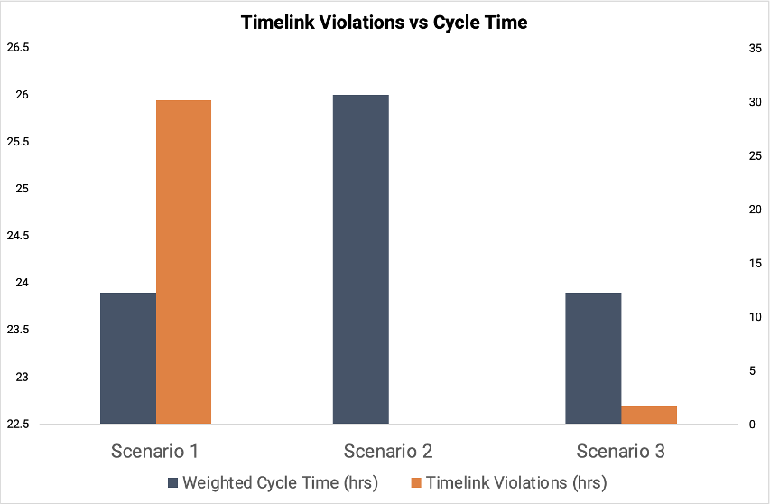
Scenario 1: Optimizing to Meet Cycle Time Objectives (Benchmark)
When purely minimising cycle time without timelinks, the priority lots are brought forward as early as possible. If timelinks were present, then the final two batches of Figure 4 would violate their timelinks.
Scenario 2: Optimizing with Critical Timelinks
In this scenario, timelinks are introduced and are all considered to be critical. We eliminate their violations, but this comes with an 8% increase in cycle time. The priority lots highlighted in light blue in Figure 4 are already within a timelink at the start of the schedule. In order to meet the critical time constraints, the lots get delayed.
Figure 4 shows the difference between Scenarios 1 and 2.

Scenario 3: Considering Timelink Criticality and Cycle Time of High Priority Wafers
In this scenario, cycle time is a vital KPI for high priority wafers. Additionally, we consider two different levels of timelink criticality; critical (should not be violated) and non-critical (can be violated if necessary). Only the timelinks feeding the final step at the furnace tool are considered critical. The critical timelink violations are eliminated first, before optimizing non-critical timelinks and cycle time simultaneously. We configure the optimizer objective so that an hour of non-critical violations would be equivalent to an hour of cycle time for the lower priority lots.
Figure 5 shows the calculated schedule when these parameters are considered; all the critical timelinks between steps 5 and 6 are satisfied, however some non-critical timelinks are broken to reduce the cycle time of the high priority lots.

Figure 6 visualises the trade-offs between timelink violations and cycle time for the three scenarios discussed. It demonstrates a benefit of advanced optimization, where different schedules can be optimized depending on the goals of the fab – whether it's purely for cycle time or adhering to timelinks.
Conclusion
Handling timelinks is crucial to managing the cost of running a fab, however it presents challenges. Our case studies demonstrate how Flexciton’s advanced scheduler can be used to plan several steps into the future when there are timelinks on bottleneck tools. Doing so helps spread WIP more evenly across tools and helps manage dynamic bottlenecks. By configuring priorities and the impact of missing timelinks, it can also flexibly trade-off violations of differing importance against each other and with other KPIs such as cycle time. This can be achieved without the need to rely on highly bespoke heuristics that are difficult to configure, require frequent maintenance and don’t necessarily guarantee the desired outcome.

With industries around the world still being hit by semiconductor shortages, chip companies need to embrace smart manufacturing practices to boost production. In this blog, we talk about what those practices are and how to accelerate their adoption.
With industries around the world still being hit by semiconductor shortages, chip companies need to embrace smart manufacturing practices to boost production. In this blog, we talk about what those practices are and how to accelerate their adoption.
Long-term capacity issues
The global chip shortage has highlighted that, despite the centrality of silicon to our technology-driven world, the semiconductor industry is far from robust. The Covid-19 pandemic may have created the perfect storm of increased demand versus restricted production. However, this is just the culmination of a long-term struggle to make semiconductor production truly agile which, alongside various geo-political factors, has now exposed the fragility of the semiconductor supply chain for all to see.
The obvious answer to the capacity issue is to build more fabs, but that’s easier said than done. Building a new chip manufacturing facility can take between three to five years, and cost anything from $4bn to $10bn. Undoubtedly more fabs do need to be built, but that isn’t exactly a quick-fix solution when the ongoing chip shortage remains a clear and present danger to industries requiring a constant, uninterrupted supply of semiconductors, from consumer electronics firms to auto manufacturers.
But that’s just to keep us where we are now – what about the R&D and production capacity needed to make the ever more sophisticated, next generation chips required to transition us to a world of ‘smart’, intelligent technologies designed to automate the environment around us and create more sustainable homes and cities? How will we get to this future if we can’t even solve the current bottlenecks that afflict the semiconductor supply chain?
Unsurprisingly, the industry itself has been attempting to address these issues, and look at ways to improve how it works. In the short-term at least, one solution to the capacity problem is to make existing facilities as efficient and productive as possible, and effectively increase capacity without having to build additional fabs.
The smart manufacturing vision
SEMI, the global industry association representing the electronics manufacturing and design supply chain, is attempting to drive this evolution via its Smart Manufacturing initiative. In a nutshell, smart manufacturing is defined as “the use of production and sensor data within manufacturing technologies to enable process adaptability”, ultimately speeding implementation and maximising efficiency. In other words, using the information generated by the factory itself to improve decision making about how best to manufacture products.
SEMI’s vision is to apply smart manufacturing practices across the entire electronic supply chain based on three essential pillars. These are:
- Sensing – establishing the state at any one time of work-in-progress (WIP) and all machines/tools within the fab, including process monitoring and location tracking
- Connecting – ensuring that all this information can be securely transferred to both internal databases and the cloud, for the purposes of creating a ‘digital twin’ of the fab
- Predicting – using the digital twin’s data, via artificial intelligence (AI) and/or machine learning applications, to optimize both WIP scheduling and available resources
SEMI is committed to promote awareness and interest in smart manufacturing practices across the industry, but acknowledges that not every semiconductor company is in the same place. While far from perfect, the industry is reasonably good at capturing data – however, the problem is that this data is often poorly integrated and can effectively become trapped in siloed systems. Without establishing a ‘single version of the truth’ by combining all data sources, it is impossible to create a functioning digital twin with which to improve efficiency.
Acceleration through disruption
To accelerate the rollout of smart manufacturing, we believe that semiconductor companies have to embrace ‘disruptive’ technologies from outside of the industry’s traditional supply chain. It should by now be standard practice for chip companies to actively seek out and adopt best-in-class technology to improve efficiency and boost output. Instead, the decision is often made to develop an in-house alternative. Operating in one of the most technologically cutting-edge industries – with a multitude of engineers and scientists at their disposal – is perhaps one reason why chip manufacturers often look inwards to find solutions to their problems. Searching internally for these complex answers can often mean years spent on researching and millions spent developing, whilst progress already made by academics and disruptive tech companies gets overlooked. The outcome is the same type of systems that have prevented the movement towards SEMI’s third pillar and properly optimizing their fabs’ processes and production.
However, in Flexciton’s experience, this reluctance is easing, with early movers already beginning to enjoy the benefits that come from a fully integrated data environment where AI-based tools can be deployed to improve and automate decision making, and help fabs to work at genuine capacity rather than the ‘false capacity’ that an over-reliance on manual processes and siloed data has created.
For companies to fully embrace smart manufacturing and truly move onto that third pillar, the next step on their journey is to transition away from conventional, heuristic scheduling software that mimics human decision-making process based on historical data. Instead, manufacturers need to adopt advanced technology that makes optimized decisions in real-time with the ability to seamlessly adapt to unpredictable fab environments. By making decisions based on the actual state of the fab and its processes in the present moment, companies can realise even more capacity and see up to 10% extra efficiency in their operations.
The chip shortage may seem like a temporary problem that will soon be resolved – but that’s a dangerous assumption. Instead, it’s a wake-up call that the semiconductor supply chain needs to be re-engineered to become fit for purpose. Fab building may be part of the solution, but more important is the need for existing facilities to be fully optimized in order to realise their true capacity – and that needs the industry to be willing to innovate and pilot cutting edge technologies.